|
|
|
|
|
|
| Topics >> by >> all_about_cmos_vsccd_sensors |
| all_about_cmos_vsccd_sensors Photos Topic maintained by (see all topics) |
||
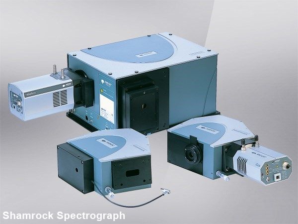
The (IUCr) Experiences with CCD detectors on a home X-ray source PDFsDevice for the movement of electrical charge A specially developed CCD in a wire-bonded bundle utilized for ultraviolet imaging A charge-coupled gadget (CCD) is an integrated circuit containing a range of linked, or combined, capacitors. Under the control of an external circuit, each capacitor can move its electric charge to a neighboring capacitor. In a CCD image sensing unit, pixels are represented by p-doped metaloxidesemiconductor (MOS) capacitors. These MOS capacitors, the fundamental structure blocks of a CCD, are prejudiced above the threshold for inversion when image acquisition starts, allowing the conversion of incoming photons into electron charges at the semiconductor-oxide user interface; the CCD is then used to read out these charges. The 4-Minute Rule for CCD versus CMOS – which performs best? - JenoptikIn applications with less exacting quality demands, such as customer and expert digital cameras, active pixel sensors, also referred to as CMOS sensors (complementary MOS sensing units), are generally utilized. However, the large quality benefit CCDs enjoyed early on has narrowed in time and since the late 2010s CMOS sensing units are the dominant technology, having largely if not entirely changed CCD image sensing units. In the late 1960s, Willard Boyle and George E. More Details at Bell Labs were researching MOS innovation while dealing with semiconductor bubble memory. They understood that an electrical charge was the analogy of the magnetic bubble and that it could be saved on a small MOS capacitor. As it was relatively simple to produce a series of MOS capacitors in a row, they linked a suitable voltage to them so that the charge might be stepped along from one to the next. Front Illuminated CCD Detector - 1044 x 64, Cooled Can Be Fun For AnyoneThey envisaged the design of what they described, in their note pad, "Charge 'Bubble' Devices". The preliminary paper explaining the idea in April 1970 noted possible uses as memory, a hold-up line, and an imaging device. The device might likewise be used as a shift register. The essence of the design was the ability to move charge along the surface of a semiconductor from one storage capacitor to the next. 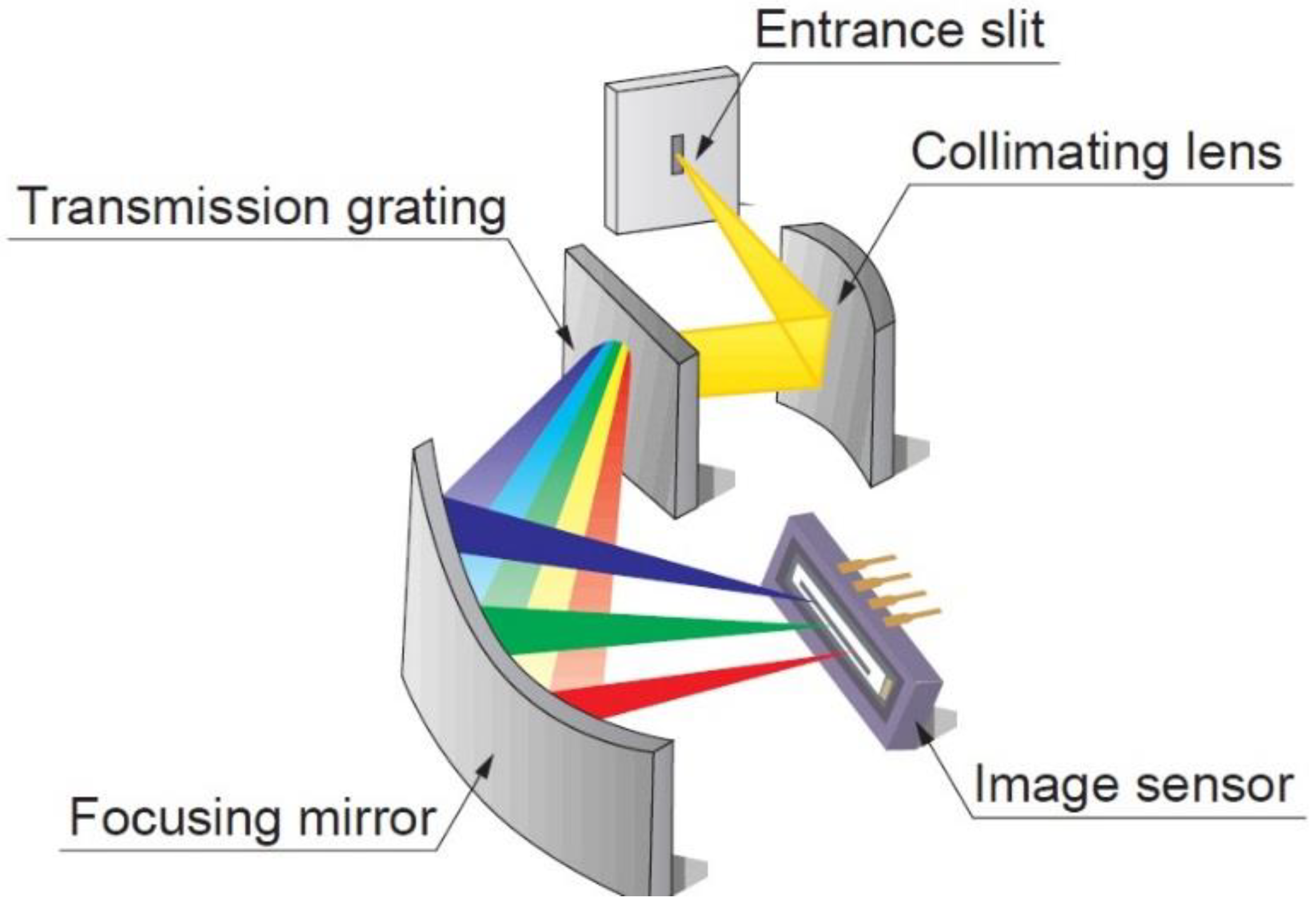 .jpg) The very first experimental device showing the principle was a row of closely spaced metal squares on an oxidized silicon surface area electrically accessed by wire bonds. It was shown by Gil Amelio, Michael Francis Tompsett and George Smith in April 1970. This was the very first experimental application of the CCD in image sensor technology, and utilized a depleted MOS structure as the photodetector. |
||
|
||