|
|
|
|
|
|
| Topics >> by >> our_the_wfc3_uvis_channel_cc |
| our_the_wfc3_uvis_channel_cc Photos Topic maintained by (see all topics) |
||
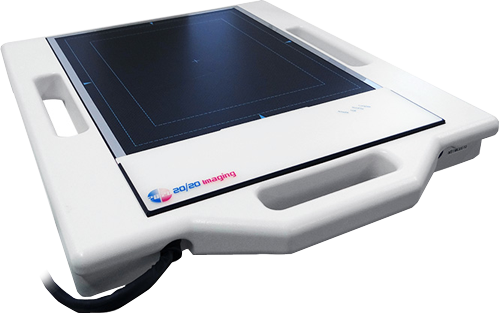
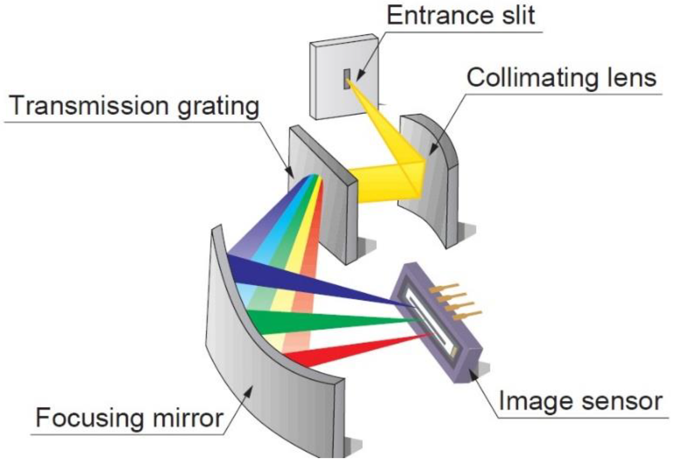 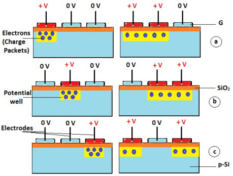 The Buzz on (PDF) Scanning CCD Detector for X-ray Powder DiffractionA one-dimensional range, used in line-scan electronic cameras, captures a single piece of the image, whereas a two-dimensional variety, used in video and still electronic cameras, captures a two-dimensional picture representing the scene forecasted onto the focal plane of the sensing unit. When the array has been exposed to the image, a control circuit causes each capacitor to transfer its contents to its next-door neighbor (operating as a shift register). By repeating this procedure, the managing circuit transforms the entire contents of the variety in the semiconductor to a series of voltages. In a digital device, these voltages are then sampled, digitized, and normally kept in memory; in an analog device (such as an analog camera), they are processed into a continuous analog signal (e. by feeding the output of the charge amplifier into a low-pass filter), which is then processed and fed out to other circuits for transmission, recording, or other processing. Detailed A Reliable Source of operation [edit] Charge generation [edit] Prior to the MOS capacitors are exposed to light, they are biased into the deficiency area; in n-channel CCDs, the silicon under the predisposition gate is somewhat p-doped or intrinsic. However, it takes some time to reach this thermal stability: as much as hours in high-end scientific electronic cameras cooled at low temperature level. Initially after biasing, the holes are pushed far into the substrate, and no mobile electrons are at or near the surface area; the CCD hence operates in a non-equilibrium state called deep exhaustion. 10 Simple Techniques For DISR's CCD detector - The Planetary SocietyFour pair-generation processes can be identified: photo-generation (approximately 95% of quantum performance), generation in the exhaustion region, generation at the surface, and generation in the neutral bulk. The last 3 procedures are called dark-current generation, and include noise to the image; they can limit the total functional integration time. In this case, the well is said to be complete. The optimum capacity of each well is understood as the well depth, generally about 105 electrons per pixel. Design and production [modify] The photoactive region of a CCD is, typically, an epitaxial layer of silicon. It is gently p doped (generally with boron) and is grown upon a substrate product, typically p++. |
||
|
||